I am using JLCPCB for my small boards. There are other places, but they seem reasonably sensibly priced, have a good automated ordering process, and are quite quick.
However, I have been trying to do something clever, and that is always a bad idea.
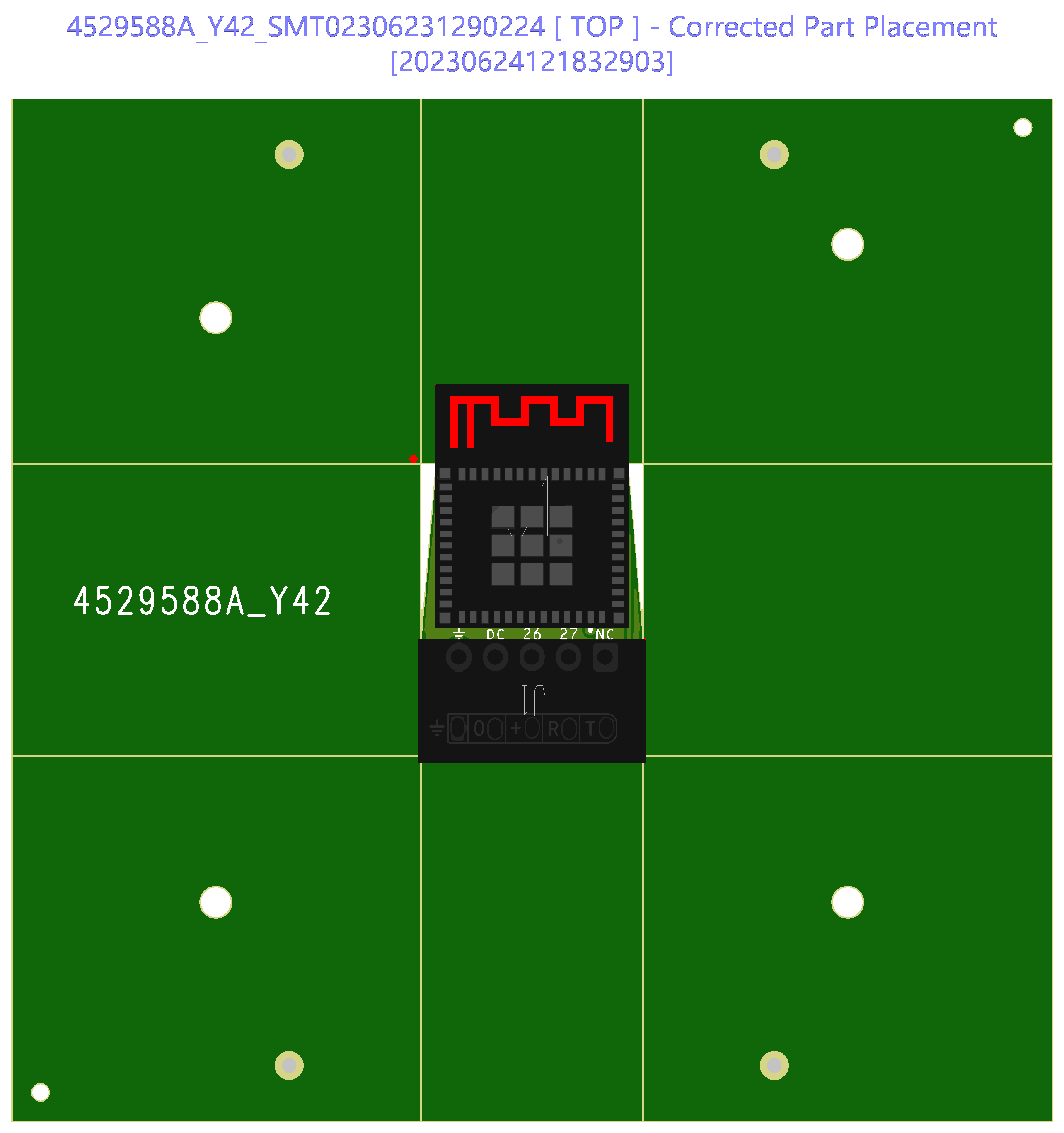
If I have a small circuit board, and want assembly, they will make it in to a small panel, e.g. 70x70m, with "rails" top and bottom, and V-cuts. This means when you get it, it snaps out of the 70x70mm PCB. The rails have some holes and fiducials.
As it happens, I am shipping (to Amazon) as a 70x70mm panel. This is partly because it fits better in a small anti-static bag, and partly to make clear it is sold as a component, an assembled PCB, and not a final product with UKCA/CE, etc. As it happens the main module is CE marked, with a RF can, and the only extra bits are normally just a small voltage regulator, so getting UKCA/CE marked should not be too hard one day, but for now, these are hobbyist projects.
Anyway, the 70x70mm panel has loads of wasted space. JLC add an order number (unless you pay them extra not to), but other than that, just unused blank PCB, a few holes, and fiducials.
So I decided to try and make use of it - make the 70x70mm panel myself. They allow this and have instructions for where to put fiducials. They also seem to want some holes and instructions seem to be lacking for those, but I copied what they did. However, this created a few challenges :-)
V-Cuts
The first problem is the V-cuts are cuts in to the board at the last stage, and always go right across the board (they explain this), but can go any direction (well, at least up/down or left/right). These allow the small PCBs to be snapped out. Some extra milling around bits of the PCB that are not simple straight edges allows other shapes, so works well.
For example, this is what they did when ordered simply as a tiny PCB. Four V-cuts to snap out.
KiCad
Firstly, how to tell KiCad. I cannot simply put these on the Edge.Cuts later as it would break the board outline - KiCad would fail DRC and not show the board on the 3D view and so on. So simple answer is a separate layer, easy enough.
But then KiCad does not know, for example, that tracks and copper fill should not get too close to these V Cuts. It knows for edge cuts, and so one can have milled slots for non rectangular edges, but the V cuts are not seen.
My solution was to make a footprint that is a 70mm V-cut.
- 70mm line on User.1 layer as the actual V-Cut
- Line on User.Comments and Fab layers to more visible
- A courtyard for 1mm above the V cut on one side
- An exclude for 0.2mm either side, front and back
The exclude keeps tracks and pads and so on away, just like Edge.Cuts.
The courtyard works on the basis that you have to bend the PCB to snap it, and that could be up or down. I have parts that hang over the edge (the antenna of the ESP32 module, etc), but by adding a courtyard one side I ensure I cannot accidentally have things hanging over the edge both sides. I have to flip the V-cut footprint to fit, but it allows a sane DRC.
Telling JLCPCB
This took a few attempts to get right.
For a start, I updated the JLC-Plugin to export an extra file for V.Cuts - I just added to the config file, and it exported. The problem though is that, even as a file called V_Cuts, it shows as a User.1 layer when viewed, and apparently this would mean adding a note to the order so they don't miss it. I don't trust myself to add a note.
However, after a few emails back and forth, I found that what they really wanted was V Cuts simply included in the Edge.Cuts file. It breaks some of the preview stuff as not a joined up border, but it is understood by their people it seems, and won't be missed.
I have done a MR on the plugin to include the User.1 in the Edge.Cuts file as part of the export, so I don't have to think about it.
Extra artwork on the panel
Adding extra artwork to the panel was pretty simple - just more silk screen. What took slightly more work is I wanted a barcode, and so made a tool to create a KiCad barcode module.
Then I ordered.
They I got a "we want $50 more" response. They said it was 3 designs. Actually, by their rules it was 5.
FFS
So, the rule is, if you have parts that detach, and they have any traces or silkscreen, they are treated as additional "designs" on the same order, and there is a surcharge for each extra design. So even a "design" that is just text on silk screen has a surcharge.
Simpler
A simple step was only silk screen on one of the unused parts, that made it 2 designs. So progress.
The problem is that the surcharge, whilst only $2 on the PCB manufacturer, they also surcharge the assembly, by around $30. Now I have queried as, even if there are 2 designs, I only want one assembled - the one with components on it.
It may be possible to order PCB as 2 designs and then order assembly as 1, but I cannot see any way to actually do that, sadly.
Solder resist
Another trick may be to avoid the multiple designs by following the rules. The rules cover tracks and silkscreen. Well, it seems we can do solder resist. Using this on an FR4 board with black solder resist may well have enough contrast. Even more so if copper fill and ENIG finish.
It needs more testing to see what resolution and contrast is achievable.
The latest attempt...
This is 2 designs because of the silk screen. But testing they agree with that by having the solder resist at the top as well.
Update: They magically decided this was 5 designs so I have challenged as "solder mask/resist" is not something they list as creating extra designs. We'll see...
Update: They seem to be doubling down on the "5 designs" still. I asked if the rules have changed?


Update: They are sticking to their rules, but making up bullshit for them, saying that they have to "load two programmes" if it is two designs. This is clearly bullshit, but I have challenged on basis that they do put their order number on silkscreen on one of the snap of panels, so extra silkscreen on that panel will be no more work, will it, as they are "loading two programmes" already, for their order number. We'll see.


With all due respect, I think this post needs a bit more work. I'm familiar with JLPCB in general but couldn't follow the details here even after reading it twice!
ReplyDelete