Showing posts with label JLCPCB. Show all posts

2024-02-19

JLPCB

As some of you know I use JLCPCB a lot for my PCBs.

Why not UK?

We do use UK manufacturers for our FireBrick products, but for the small cheap PCBs I make, it is simply not viable. I have tried to get competitive quotes but people in the UK cannot match the prices, or even close, or the time scales. It is a real shame, and would be great if the UK could find any way to compete.

Problems?

I posted about a weird tracking issue a while back. Thankfully it was a one off.

But things have gone down hill.

Stupid rules

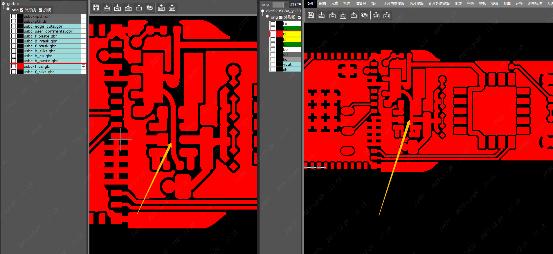
One issue (I don't think I posted) was that they charge a surcharge for "multiple designs" on a PCB, i.e. where cuts or v-cuts allow parts of the board to be broken off, and those have different designs on them. I don't follow the logic at all. But what is even more weird is the logic for this - any tracks or silk screen on break of parts makes it a different part. If just blank, it not and so no surcharge. They can silk screen on it at no extra (e,g. their job number). I even tried to "follow the rules" and had text done in the solder resist (they say explicitly tracks and silkscreen as separate parts, not solder resist), but they would not play. It is a shame, I just wanted a bar code (for the board) on the break of parts of a panel. Pain, but their stupid rules.

Broken search

More recently I found, when uploading, a part was not in stock, a 124k 0402 resistor. For a start, how is that not in stock, but I did the search option and it showed many 0402 parts and I picked one in stock.

What fooled me is the search did not list resistors matching the value I was searching, and I managed to pick a 0.124Ω resistor. My mistake, after a broken search, and I got a UK company to rework for me ("hot tweezers").

Broken component selection

Anyway, my mistake. This time I ordered more boards, same bill of materials I have used dozens of times before, and for this one component, the same as dozens of designs of boards over the last 6 months.

The BOM has an "R" (i.e. resistor) in an "0402" package, with a value of "124k", simple. I don't care the other aspects, it is a potential divide as a reference for the regulator, so really does not matter what 0402 124k resistor it is, hence I have not picked a specific LCSC part number for a specific manufacturer, as that could be out of stock more easily. Like simple resistors and capacitors I simply list the value I want, obviously.

As usual, it picked the parts, and showed them, not actually showing the value, as truncated. But I gate it a value, as I have done so many times before, and obviously expect it to pick a resistor of that value.

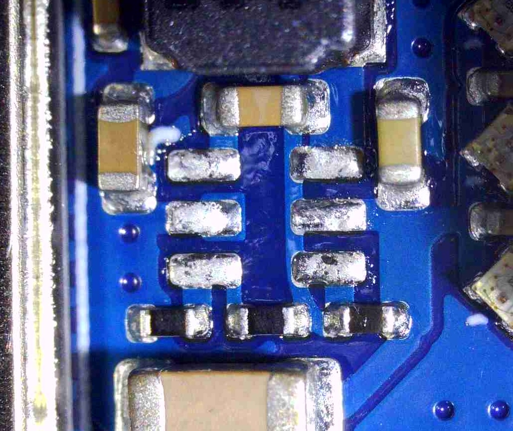
Suddenly, this time, it picked a 1.24Ω resistor. So ignored the value I specified! This happened on two orders. One I will have to pay someone to rework, again!

This is bad, I should be able to just say I want an 0402 resistor of a specific value and it pick one. That really is one of the most basic things they can handle in the BOM upload. They used to handle it.

Update: Just to be clear, I have used JLC for years and never had an issue until now, but now it is seriously broken. I re-tested, and even adding Ω to the value does not help. Magically today the 124k is working, but the 1M is suddenly 51kΩ - which makes no sense at all. Previously perfectly fine BOM files now fail randomly. I tried setting specific LCSC parts, which works, except that they are then out of stock of the specific parts and you have to search parts instead of just using a known working BOM.

Baking

And now the latest fiasco, and this really is now taking the piss,.

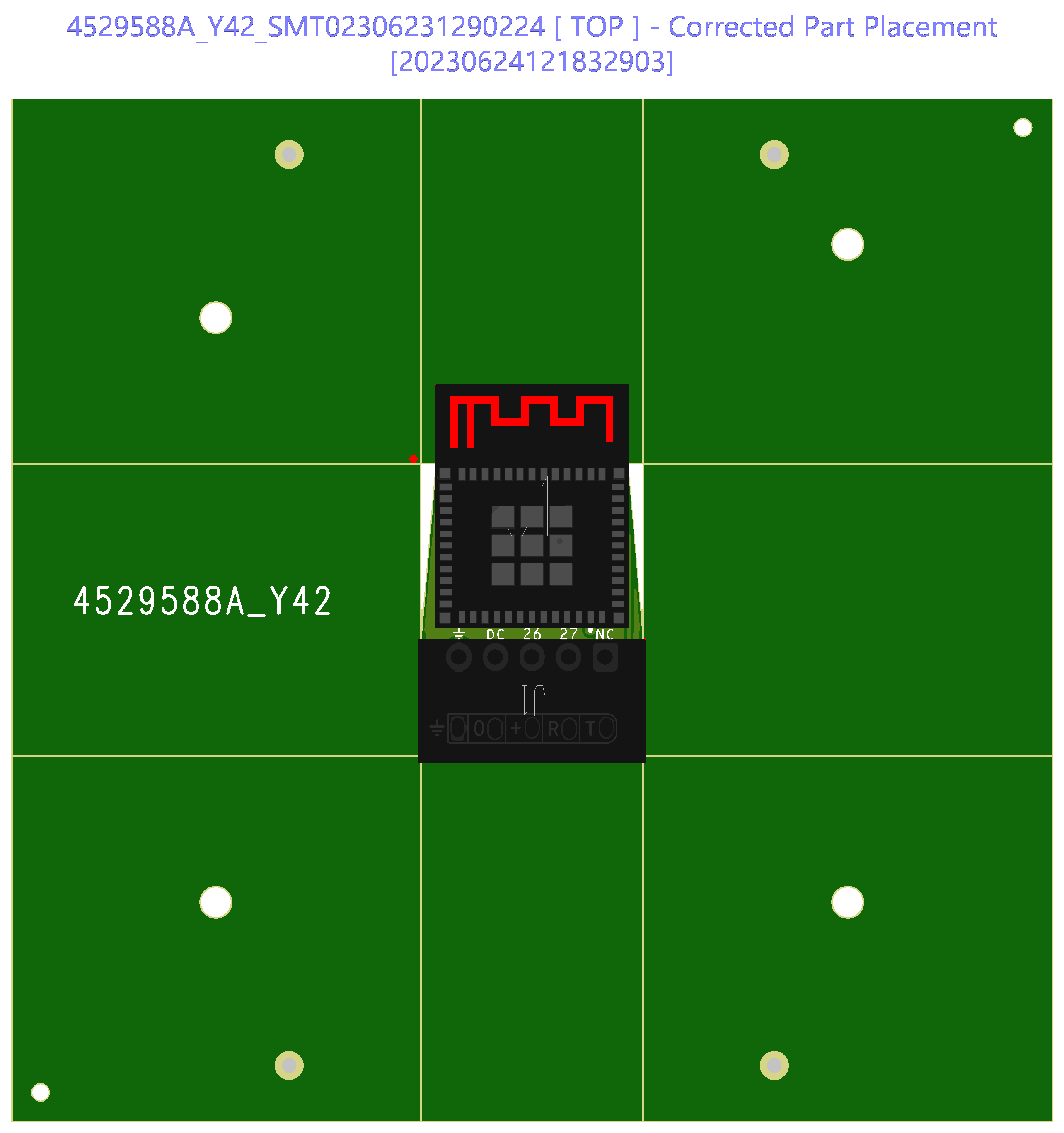
A part I have used on dozens of designs over at least 6 months, and hundreds of boards. A simple LED. Indeed, my Stargate designs actually have over 500 of them on each board!

The design I am ordering is one I have ordered many times, indeed, I just received some I ordered over a week ago, same BOM, same LED (wrong resistor, as above).

But now, for some reason this "is highly sensitive to humidity, and needs baking before soldering, or it will easily got moisture damaged". They suggest checking the datasheet. There is a surcharge!

The datasheet says: "If the moisture absorbent material has fade away or the LEDs have exceeded the storage time, baking treatment should be performed based on the following condition: (60±5)°C for 24 hours."

This suggests they have stored it incorrectly maybe? and want me to pay a surcharge for their bad handling of a component.

Awaiting reply, but they have gone from "quick, easy, cheap", to "pain in the arse, costly rework, and stupid rules and extra cost."

I may have to find someone else!

2023-12-28

Ordering PCBs

Ordering PCBs and assembly is fun :-)

Well, not fun, and to be honest, one of the biggest challenges is the parts selection, what they have in stock or something equivalent, but designing the PCB is definitely fun (well, for me).

I export a gerber files that are the instructions to make the PCB tracking images, and also a BOM (bill of materials) and position file, for placing the parts.

I have done this many many times with several PCB manufacturers, and lately with JLCPCB, which seem to be surprisingly quick and sensibly priced (apart from the odd quirk). I'd love to find a UK company as cheap and easy to use, I'd use them.

The PCB printing has a few design constraints, the gaps between tracks, minimum track width, and so on, which relate to the optics of the process for printing and drilling the board itself. But apart from that the PCB is printed exactly as expected.

Well, until now.

This is what I ordered... (this is an image from their order history page)

And this is what arrived...

It took me ages to debug it - tracking down that the CPU was running way too hot (burned my finger) and not quite right. It turned out it was running on 4.5V not 3.3V. The shorts there short input to output on a regulator circuit and I was testing from 5V USB via a diode. If I had tested 12V it would have made smoke, I expect.

The thing is the order process involves a lot of steps, and each step show the PCB you are making.

  • When uploading the gerber files
  • When selecting assembly and it shows the bare PCB
  • When showing PCB with parts
  • When order complete and preview of PCB
  • When order complete and preview of assembly
  • On gerber viewer on the site from their order confirmation

At every stage they show the circuit correctly, but the final PCB was faulty.

I complained, and they advised: "We have reflected this issue to our engineering team and JLCCAM software team and they have found and fixed the issue just now, and there will be no the same issue next time, so don't worry about it."

They even provided an image of the error:

Next step - refund!

My view is simple.

  • They made an error in printing the PCB.
  • Arguably they made an error with the flying lead test of the PCB not spotting the printing error.
  • They then made the PCB with parts that cost money - either of the above errors not made would have avoided that.
  • It was not, in any way, my fault.
  • I did not get what I paid for.

It is simple. I should not only have a full refund, including shipping cost, but ideally I should be compensated for the hours of debug, the delay in getting working boards, and the cost of disposing of the WEEE (defunct PCBs and part).

I'll be happy for just a full refund, and either they pay for courier to return boards, or I dispose of them (at my cost). As I buy loads from them, I'd even allow for it to be a credit on my account rather than an actual refund.

I have a funny feeling they will try and weasel out of this - and then I may have to ask Amex to intervene. It is for two separate batches of boards (from 4 I ordered, 2 of which were fine) totalling over $470.

Watch this space - I'll update with news.

Update: They do seem to be trying to weasel out of out - that PCB manufacturer is separate from supplying parts and assembly - but the parts they supplied are useless to me as supplied, so not reasonable that I pay for them, surely? Indeed, I have offered to send the parts back to them (at their cost). We'll see how that goes.

They suggested I try and isolate the track, but this is cutting through soldered pads, so when I put the components back it will short again!

Update: They are being counter reasonable. I suggested I could maybe find someone to rework - they suggested I try, and get a quote. I may try and get a quote.

They also think just cleaning solder would be enough to avoid shorting with the component leads when cut like this...

Update: I have decided instead to offer a compromise on basis that on one board I can re-use the SCD41 sensors they have supplied. Pushing their offer $50 more on each set of boards. We'll see.

Update: We have credits now.

2023-09-27

Dialling the gate

People will know I am a slight Stargate fan (!), and I like making PCBs. So, well... Latest is...

LEDs

First off, the LEDs. There is a very popular LED format, a WS2812B chip and RGB LEDs in a package. These use a serial daisy chained control channel allowing 256 colours of each of Red, Green, and Blue, to be loaded individually to a whole chain of LEDs. This design has 372 LEDs.

There are standard libraries to drive these, but I have discovered the ESP32 S3 is better as it uses DMA for the "remote control" hardware that is used to drive the data for these LEDs.

You can get these on tapes, and rings, and so on, usually 5mm x 5mm, or 4mm by 4mm, and I had even seen some 2mm x 2mm, but was surprised to find they are now available in these tiny 1mm x 1mm format. This ring design has a 100mm diameter centre hole.

They also usually need 5V power, but amazingly these small 1mm x 1mm modules work on 3.3V (or 5V), which is impressive (Blue is usually the voltage hog).

They are also very cheap. Part XL-1010RGBC-WS2812B, LCSC Part C5349953.

Alignment

My first mistake with the LEDs was making the layout simple, so a grid of these LEDs were one way up on one row, and the other way up on the next row. This allowed GND to be between two rows, then VCC between two rows, and so on. I put caps at the ends of the rows (which works well). This allowed me to pack them at 1.6mm spacing.

This was impressive, but I missed the (apparently well know) issue that the LEDs are placed within the 1mm x 1mm space, so for example Red is one side, and hence an all grid red looks like this, not evenly spaced.

They have to all be the same way around to avoid such issues.

Diamonds

I tried doing the same way and really a pain to track. The trick is to actually place them at 45 degrees, diamond style. This makes tracking really simple.

This allows a track at the top for GND, and at the bottom for VCC, and a link from LED to LED corner to corner for the daisy chained data line. Shown here I have vias for extra power. With thin tracks between the pads of the capacitors (expected to be one per LED) it makes for a really neat layout.

Grids

Grids were easy, and grids of LEDs like this are simple, with 2mm spacing (no caps), which is not bad. Caps added at end of row or column.

Apart from tracks joining VCC and GND top and bottom, or side and side, I actually created zone fills to make for thicker overall power tracks.

The latest design at 2mm spacing is 10mm x 18mm for a 5x7 grid, and allows them to be placed next to each other for a whole row at 2mm spacing, LEDs at the top and bottom of each column.

Rings

The other thing to do was rings of LEDs.

The principle is pretty simple, tracks (this time arcs) for GND, data, and VCC. Some zone fill for VCC and GND, again arcs (well polygons and lots of points).

Adding vias is fun, and I ended up with code that puts them off to one side if diodes and caps too close together (as above image) or in line in the GND/VCC tracks when enough space.

A simple ring with evenly spaces LEDs and caps is easy, but then I decided I needed some grouping of LEDs together with specific tighter spacing (the chevrons in the top image).

I also had to cater for the fact that power vias from one ring could clash with some of the next ring, and so omit some that were too close.

C code

If you have tried doing this in KiCad, it is far from easy - even with the grid locking and simple spacing like 2mm, it is hard, and making a ring with 39 LEDs, i.e. 4.6153846 degrees between LED and cap and LED, is, well, totally impossible. No chance doing it manually at all.

So, obviously, I ended up making C code, parsing in the PCB file, and moving LEDs and caps and making tracks and vias and fill zones. I have code for grid layout and ring layout now.

The gate

Working out the exact animation for the gate will need a bit of trial and error I expect - I cannot actually spin the symbols, so some poetic licence involved, but easy to "spin" the rings of 117 LEDs.

I have actually gone for a number of rings...

  • 117 inner rings, this is 3 per gate symbol, so makes for a nice "1 in 3" spin effect and allows the inner to be lit up and made sparkly for the gate open.
  • 39 gate symbol ring, so I can light individual symbols during dialling (seeing as they don't spin).
  • 18 ring for bottom of engaged chevrons (9 chevrons, so 2 per chevron).
  • 117 outer ring, again for spinning, but also can be two for chevron when engaged, and 3 for chevron end when not.
  • Two 18 rings for chevrons getting wider.
  • A 45 ring, so 5 per chevron, for the lights at the edge of the gate when selected.

I think making it dial will be cool. PCBs ordered, so a week or so (maybe more, some holiday in China), and I can post video of the real thing.

Open source

This is all open source, PCB designs and code, but if you want to buy one of these, and a driver, let me know. I have 5 on order.

2023-06-29

Pipelining

I am reminded of years gone by when "compiling" would take a long time, even hours in some cases.

This lead to a "pipelined" debugging and development cycle. By the time what you did was compiled you already had fixed a load of bugs and added a load of new features that needed testing. So you had to test things from the compilation as they were when you started. Sometimes you just knew the compilation would create something broken, but some other aspects would be things you need to test, so you let it run anyway to test them. You had to make code that would include things you need to test in the best way possible.

I am sort of doing that with PCBs over the last week or so - getting a new PCB takes slightly over one week from China.

I have been working on a load of small changes to various designs.

  • New 5 pin pad for programming - I made a larger set of holes as the ones on my last batch were annoyingly small and have to be held in place while programming. This is one I finally have back prototypes and my new design is too big and loose, FFS.
  • New New 5 pin pad for programming, staggered more than last time to allow pins and hold them whilst programming - waiting - works perfectly
  • New voltage regulator - waiting - and I really hope it is right as I have several in the pipeline with no fallback - one version works nicely (the cheaper one), the other (tantalum cap) does not work.
  • New USB UART - got a board, discovered I cocked up - but was able to rework some and test the correct design - some boards were able to be used anyway
  • New New USB UART - fixed layout/design issue - waiting - working
  • New RGB LED - waiting, but already spotted that I have cocked up and got G and B swapped, FFS. This means the resistors will be wrong for the colours as well. May be able to rework when this arrives.
  • New New RGB LED - waiting on revised, but still not been able to check if resistors right - waiting - working
  • New panel design - i.e. making part in a 70x70 panel instead of JLC doing it, and if a barcode is clean in silkscreen - waiting - looks nice but JLC being a pain
  • New Tx on Faikin, open drain output - waiting - working
  • New Rx pull to 3V3 on Faikin, detect loopback - waiting

The whole thing is frustrating. I have had to scrap one set of boards sadly because of the CH340X issue. Others I was able to rework, or remove and use a 5 pin programming header instead. One trick is making a new board that you can "fall back" if the new bit does not work.

The RGB LED is a pain - I used one (side mounted) that worked nicely because they did not have the simple one I got from Mouser and used for my hand soldered boards. But JLC places it badly (over 10% of boards needed rework). And I found they had an equivalent simple front facing RGB LED with low enough voltage on the blue for 3.3V working. The issue is the resistors - you can work out values - as I had originally but then find green is way too bright. For my manual working I had changed resistors and so am trying those values to start with. But until I get them, and get the G and B right, I will not be sure I have the right resistors even if I have the right colours. I may have to rework some 0402 resistors to test when they arrive.

On top of it, DHL, who have managed around 2 days from China with no VAT issues, have suddenly made it 3 or 4 days and not doing proper VAT with postponed VAT accounting - that will be a fun argument as I am planning to refuse to pay and insist they re-do as PVA. We will see.

Also JLC being odd on rules, insisting multiple designs on a board even if only in solder resist. Still not resolved. Even if I end up making panels with no extra silkscreen, at least making as panels myself, instead of leaving JLC to do it, lets me make cleaner slots and edges on the designs.

I have to test if the barcode in silkscreen works, and is acceptable (inside a nearly clear, slightly pink, anti static bag) with Amazon - so avoiding having stickers.

So a very frustrating week, and another such week to come.

2023-06-28

JLCPCB and fun rules

I am using JLCPCB for my small boards. There are other places, but they seem reasonably sensibly priced, have a good automated ordering process, and are quite quick.

However, I have been trying to do something clever, and that is always a bad idea.

If I have a small circuit board, and want assembly, they will make it in to a small panel, e.g. 70x70m, with "rails" top and bottom, and V-cuts. This means when you get it, it snaps out of the 70x70mm PCB. The rails have some holes and fiducials.

As it happens, I am shipping (to Amazon) as a 70x70mm panel. This is partly because it fits better in a small anti-static bag, and partly to make clear it is sold as a component, an assembled PCB, and not a final product with UKCA/CE, etc. As it happens the main module is CE marked, with a RF can, and the only extra bits are normally just a small voltage regulator, so getting UKCA/CE marked should not be too hard one day, but for now, these are hobbyist projects.

Anyway, the 70x70mm panel has loads of wasted space. JLC add an order number (unless you pay them extra not to), but other than that, just unused blank PCB, a few holes, and fiducials.

So I decided to try and make use of it - make the 70x70mm panel myself. They allow this and have instructions for where to put fiducials. They also seem to want some holes and instructions seem to be lacking for those, but I copied what they did. However, this created a few challenges :-)

V-Cuts

The first problem is the V-cuts are cuts in to the board at the last stage, and always go right across the board (they explain this), but can go any direction (well, at least up/down or left/right). These allow the small PCBs to be snapped out. Some extra milling around bits of the PCB that are not simple straight edges allows other shapes, so works well.

For example, this is what they did when ordered simply as a tiny PCB. Four V-cuts to snap out.

KiCad

Firstly, how to tell KiCad. I cannot simply put these on the Edge.Cuts later as it would break the board outline - KiCad would fail DRC and not show the board on the 3D view and so on. So simple answer is a separate layer, easy enough.

But then KiCad does not know, for example, that tracks and copper fill should not get too close to these V Cuts. It knows for edge cuts, and so one can have milled slots for non rectangular edges, but the V cuts are not seen.

My solution was to make a footprint that is a 70mm V-cut.

  • 70mm line on User.1 layer as the actual V-Cut
  • Line on User.Comments and Fab layers to more visible
  • A courtyard for 1mm above the V cut on one side
  • An exclude for 0.2mm either side, front and back

The exclude keeps tracks and pads and so on away, just like Edge.Cuts.

The courtyard works on the basis that you have to bend the PCB to snap it, and that could be up or down. I have parts that hang over the edge (the antenna of the ESP32 module, etc), but by adding a courtyard one side I ensure I cannot accidentally have things hanging over the edge both sides. I have to flip the V-cut footprint to fit, but it allows a sane DRC.

Telling JLCPCB

This took a few attempts to get right.

For a start, I updated the JLC-Plugin to export an extra file for V.Cuts - I just added to the config file, and it exported. The problem though is that, even as a file called V_Cuts, it shows as a User.1 layer when viewed, and apparently this would mean adding a note to the order so they don't miss it. I don't trust myself to add a note.

However, after a few emails back and forth, I found that what they really wanted was V Cuts simply included in the Edge.Cuts file. It breaks some of the preview stuff as not a joined up border, but it is understood by their people it seems, and won't be missed.

I have done a MR on the plugin to include the User.1 in the Edge.Cuts file as part of the export, so I don't have to think about it.

Extra artwork on the panel

Adding extra artwork to the panel was pretty simple - just more silk screen. What took slightly more work is I wanted a barcode, and so made a tool to create a KiCad barcode module.

Then I ordered.

They I got a "we want $50 more" response. They said it was 3 designs. Actually, by their rules it was 5.

FFS

So, the rule is, if you have parts that detach, and they have any traces or silkscreen, they are treated as additional "designs" on the same order, and there is a surcharge for each extra design. So even a "design" that is just text on silk screen has a surcharge.

Simpler

A simple step was only silk screen on one of the unused parts, that made it 2 designs. So progress.

The problem is that the surcharge, whilst only $2 on the PCB manufacturer, they also surcharge the assembly, by around $30. Now I have queried as, even if there are 2 designs, I only want one assembled - the one with components on it.

It may be possible to order PCB as 2 designs and then order assembly as 1, but I cannot see any way to actually do that, sadly.

Solder resist

Another trick may be to avoid the multiple designs by following the rules. The rules cover tracks and silkscreen. Well, it seems we can do solder resist. Using this on an FR4 board with black solder resist may well have enough contrast. Even more so if copper fill and ENIG finish.

It needs more testing to see what resolution and contrast is achievable.

The latest attempt...

This is 2 designs because of the silk screen. But testing they agree with that by having the solder resist at the top as well.

Update: They magically decided this was 5 designs so I have challenged as "solder mask/resist" is not something they list as creating extra designs. We'll see...

Update: They seem to be doubling down on the "5 designs" still. I asked if the rules have changed?


Update: They are sticking to their rules, but making up bullshit for them, saying that they have to "load two programmes" if it is two designs. This is clearly bullshit, but I have challenged on basis that they do put their order number on silkscreen on one of the snap of panels, so extra silkscreen on that panel will be no more work, will it, as they are "loading two programmes" already, for their order number. We'll see.

2023-05-10

TX1812Z5 and WS2812B

I have used the classic WS2812B LED strips, they are very common, and AdaFruit do a lot.

They have a serial data line, in and out, on each RGB LED, and GND and 5V, making them ideal to make an LED strip will all programmable LEDs.

They work by sending a serial stream of short+long or long+short bits, 24 bits per LED, so the first LED "eats" the first 24 bits and then passes on the rest. A gap then means all done and they can all load the LED pattern. The data is around 1.25uS per bit, so even with hundreds of LEDs, this is really fast to update.

There are standard drivers, including for ESP IDF on the ESP32s I use.

But, try as I might, I could not find any of these common 5mm x 5mm "neopixel" RGB LED modules on LCSC/JLCPCB for an LED ring project. They had them on LSCS, and in stock, but would not pick up on a BOM on JLCPCB, or even allow a parts buy from LCSC, crazy!

What they did have is a much smaller, 2.1mm x 2.1mm, TX1812Z5 based, modules. And a Chinese data sheet!

So, tentatively, I designed boards using these and ordered. They are smaller, which is nice. The design was fun, C code to make circular tracks...

I was lucky - JLC queried the pin 1, as I did not (originally) have any pin 1 mark on silk screen, and only then did I realise the pin numbering for the 4 pins was different to the common 5x5 LED modules. So I was able to cancel the order at that point. Had that not happened I would have a number of duff boards!

Having got the pin out right, I ordered again. Then I had a slight panic. The LEDs are run on 5V, and hence a USB lead feeding the inner ring as 5V there. For 24 LEDs in the ring a USB-C will be fine. But, I spotted in the Chinese data sheet that min VIH is 0.7VDD which would be 3.5V, and I am driving from 3.3V data line as that works with a normal neopixel module. It was too late to cancel. But to be fair, WS2812B says 0.7VDD as well, and I know that works with 3.3V.

I also spotted that the timing was 295ns and 595ns not the timing for WS2812B which is 400ns+850ns or 800ns+450ns. Thankfully this would be easy enough to fix in software.

To my surprise, it just worked. The only issue was my PCB sandwich design is a bugger to solder the boards together. Timing and voltage do not seem to be an issue!

The project is a PCB sandwich, with top being a coaster for an (empty) fancy bottle on each table at a wedding. It is going to be awesome.

2023-01-19

Assembled PCBs from China

I have been using JLCPCB to make PCBs for a while. This is for some of the smaller PCB projects at A&A (here), rather than the big projects we do for FireBrick. It means I am learning a lot.

This month I decided to try and have some "assembled" PCBs done. They have a quite nice ordering page allowing you to view the assembled board. This is important as it seems components have no standard for the reference point, nor rotation, and it varies from PCB manufacturer to PCB manufacturer. The tool I found for KiCad is excellent (here), but I did have to make from the GitHub page, rather than using the library/plug-in manager, as that was out of date. Importantly it allows me to add "offset" and "rotation" adjustments needed for placement of parts. That way I can make working production files in one click, which is amazing.

The big challenge in updating various designs was finding parts - the parts they have available readily, without ordering in, are all very similar to what I am using, but often I have to hunt down the right part number. In one case I found that an inductor was not available in the same package, only to find it was if I did not add a part number. Somehow their search found it even though I failed to. The bigger annoyance was the RGB LED I am using, which is low enough voltage to work from 3.3V. They had a load that are the same footprint even but not the low power and low voltage. I ended up using a different part, different footprint, and even sideways mounting, meaning changes to layout, albeit minor.

I still have to work out how to handle some missing parts - the SCD41, for example, around £30, but they (a) have no stock, and (b) list as $150. So that would not be fitted, and I would have to fit. I am wondering if I can put on the soldered pads with some flux and run through the oven I have. I'll have to test that.

However, for the first board to test the process I ordered the simple Shelly Tasmotizer (here). It does not have a processor, but does have two hand soldered connectors, which was also a good test. They ended up costing £19+VAT each, for a 10 off run, including shipping and assembly and parts. They get a lot cheaper if you order more, of course.

They arrived, and, well, just work. They look really neat. I am impressed.


QR abuse...

I'm known for QR code stuff, and my library, but I have done some abuse of them for fun - I did round pixels  rather than rectangular, f...