Milling PCBs
As some of you may know, from previous blog posts, I got quite good at milling PCBs. Basically, if you want to make small circuits at home, one option is a milling machine.
It does have some key advantages - the main one being time. You can have an idea in the morning, and design a circuit, layout a PCB, mill it, and have it soldered and working by lunch time. You can do several iterations of a board during a day. Another advantage is the cost - just the cost of the copper clad board, and the occasional new drill bit.
However, there are limitations. The main issue is that is it single sided - whilst a double sided milled board can just about be done, it is hard to align and the holes are not plated, so need links. The accuracy is an issue too - using a USB-C connector was just at the limit of possible, mainly as I only needed to connect two of the smaller pins (CC1/CC2), and even then - the more detail you try and do, the harder it is to get right first time.
So, moving on - what else is there? What I am doing is not quite hobby, it is more R&D, so I need slightly better than just milled board. The answer is getting fast turnaround PCBs professionally made. The nice thing is that double sided and plated through hole now becomes the norm.
KiCad
But before I could get boards made, I needed a new way to design them. For milling boards I was using inkscape to lay out the milling path. That was not going to cut it when someone wants Gerber files. So I asked Twitter, and several people suggested KiCad - a free package that was available to run on my Mac.
It is nice, I have to say. It does the schematic, and then one button and you are in to PCB layout. It has design rule checks at each stage. The PCB layout is nice - I worked out that I prefer the "push" mode where running a new track which pushes the existing ones out of the way. It has limitations, but makes it easy. The other trick I did not realise initially is I can redraw an existing track in a new direction and it will remove the original part I have now bypassed, allowing more major track moves than "push" can handle, and making it easy to do cosmetic tidy up at the end.
It also does a lovely 3D view, and it seems that not only does its built in library have 3D models for lots of things, most components have them available as standard now. Even complex modules like the Pololu D24V5F3 regulator has one. I was able to add new parts at schematic, footprint, and 3D model without any real problems.
And, of course, it will simply make Gerber files and Excelon drill files, at the click of a button.
It is also rather nice being able to design for double sided with fine tracks - it makes it way easier to track boards and allows me to make a much smaller board.
PCBTrain
So, I sent the Gerbers to PCBTrain. And two days later, they arrive. they look good.
They look nice. They are their quick turnaround product, which is copper with silver, and no solder resist or silk screen, but they work.
I even got good at soldering things like the USB-C connector.
The trick was lots of flux, and a good soldering iron. Tinning the pads first and then just heating the pin to fix it. It takes a bit of practice :-)
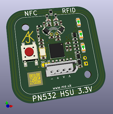
Tiny ESP32-WROOM-32 board
My first project to test the whole process was a minimal usable ESP32-WROOM-32 board. The idea was a board with USB-C or DC power, several GPIO on a connector, and built in serial for programming. The challenge was to make a small as possible. I think it came out well.
The result is tiny. But with 5 GPIO pins it is very flexible for all sorts of IoT applications. There is no way I could have made this on a single sided or milled board.
I also made each GPIO have pads for a pull up resistor, or, if powering something from the connector, a zero ohm link. This works well for things like a DS18B20, but could be connected to all sorts of things like an RFID reader, a GPS module, or whatever. It has enough pins that this module could run my ASR33 teletype, and be a lot smaller and neater than the node-mcu board I am using now (so that may happen).
One nasty hack was the USB connector I am using is through hole - as that makes it a lot more robust (their is nothing more annoying with these than pulling the connector off the pads by mistake). To do this I ended up with holes going through 4 of the GPIO pads on the ESP32 module. But it has a lot of GPIO, and they default to input, so no problem, as long as the software knows not to use them. Obviously I had to tell the schematic that they were grounded too.
Another trick was the the Pololu module was not fitted using pins. I could use pins and clip them short, but as it happens, with the through plated holes, just solder down the holes secures it nicely. I only use 3 of the 4 pins, as that would have put a pin through the ESP module pads too, and not in a good way this time. I did have to remember to put a pad under the 4th pin else it ended up on a GND fill which would have been bad.
The end result really is quite small.
FTDI FT230X USB/Serial
The final new bit for me was building in serial for programming. Previously I had made designs using a 4 pin SPOX connector which connected to a serial/USB lead. This takes quite a bit of board space. So I investigated serial USB chips. FTDI seem to be the king of serial USB, and they do a small 16 pin QFN-16 package module, the FT320X. I checked some videos of people soldering QFN packages by hand, and figured I'd be able to.
It is a nice small chip, connects to USB, and provides serial with Tx, Rx, RTS, and CTS as well as 4 configurable CBUS pins. It even has a 3.3V regulator, though sadly not enough to run the ESP32 - that would have been awesome!
There is one small downside - it needs a few passives. That is a pain on a small hand soldered board, and where I am trying to make it tiny (just for fun), so I built without the passives. This will mean the USB is not properly impedance matched. But it is good enough for programming in my tests, and that is all the serial lead is actually for. So what the hell? OK, yes, it annoys me to cut corners even on a fun board and I may try to at least squeeze the 27R series resistors at some point. I am not normally one to cut corners.
However, the small size, and passives, were not the only issue. I decided to connect RTS to the EN (reset) pin on the ESP32. This is a common trick and the tools, like the ESP IDF flash tool, pull RTS low and then high to reset. It is risky in a way as a "normal" serial port will make RTS low when ready for the ESP to send data, but it seems the common tools do not, so it works. What I was unsure of until I tested is that this pin stays high when otherwise idle, and when connected just to power and not a USB driver, and so on. It does. It works. Yay!
However, to program an ESP you need to put in to boot mode, and this means pulling GPIO0 low during reset. Most boards have a button for this which you have to hold when programming. Apparently some do a trick with DTR, including the ESP IDF flashing tools.
Snag! There is no DTR on the FT230X. What is extra weird is that DTR is not one of the CBUS pin modes, so you can't even create a DTR. This seems an oversight as other FTDi chips have DTR, DSR, DCD, and RI, so why are they not options on CBUS pins? Why does this matter? - well a normal serial driver will be able to control RTS and DTR as they are standard pins. To control special pins like CBUS on the FTDI needs code written specifically for the FTDI, not just any serial connection. So not using DTR makes it "special".
I considered just adding a button, but a bit more research has led me to use CBUS0. The problem then is how do you use CBUS0? It has multiple functions (not DTR, sadly), which can be configured.
FTDI EEPOM
The answer is that you programme the EEPROM in the FTDI chip. This lets you set a manufacturer, description, serial number, PID/VID, and a load of settings. One such setting is what each CBUS pin does. One of the options is a GPIO. So that is all I have to do - zap the EEPROM with the right data.
Snag! There is a tool, ftdi_eeprom, that is simple to install on a Mac. But it only lets you set a few things from a config file, and not CBUS functions. And even though it will read the EEPROM to file, it won't just write a file to the EEPROM - it insists on "building" it from your config, even bits you might have deliberately set in the file, like CBUS functions. Arrrg!
So I ended up making a tools, ftdizap, which allows me to simpley set certain (well, any) settings in the EEPROM. I also made it work the CBUS pins when set to GPIPO mode so it can control the output on the CBUS pins directly as a command line tool.
This means I can flash by using ftdizap to set CBUS0 low, then running make flash, then setting CBUS0 high and resetting with RTS low/high. It works on my Mac and on my linux machine. So, simples. A minor tweak to the make file, and I can simple make and flash new code in one go - no button pressing. The make monitor also works, leaving RTS high, allowing debug.
I also set the other CBUS pins to various modes and connected to GPIO on the ESP32. This allows the code to tell if in a "charger" mode, or if simply "not connected to a USB host", or if "put in to USB sleep mode". All of which could be useful in some circumstances.
What next
I already have another board design - this one slightly more useful. It is a small board the same size as a 1.5" RGB OLED display modules (commonly on Amazon). It fits all the necessary components between the board and the display, including a USB-C socket, and the FT230X. It has an 8 way SPOX socket so providing 7 GPIO pins. It has pads for DC power alternative to USB power. It also has pads to allow an SCD30 CO₂ module to be fitted to the back to make a complete environmental monitor. The pull up resistors on the GPIO allow it to be set up for a DS18B20, and the choice of SPOX sockets allows for a 3 pin SPOX plug connected to a DS18B20 to go in to the 8 pin SPOX socket nicely. It should make for a very flexible board.
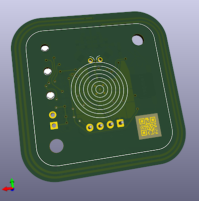
As you can see KiCad does a nice rendering of what it will look like.
Published?
Yes, the code, and the boards, are all on my GitHub. Just bear in mind that they are likely to have several updates over the next few days.