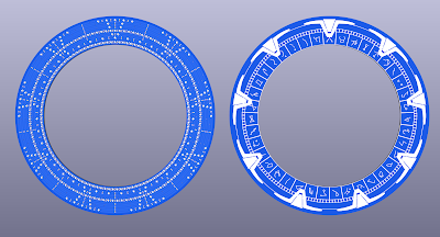
People will know I am a slight Stargate fan (!), and I like making PCBs. So, well... Latest is...
LEDs
First off, the LEDs. There is a very popular LED format, a WS2812B chip and RGB LEDs in a package. These use a serial daisy chained control channel allowing 256 colours of each of Red, Green, and Blue, to be loaded individually to a whole chain of LEDs. This design has 372 LEDs.
There are standard libraries to drive these, but I have discovered the ESP32 S3 is better as it uses DMA for the "remote control" hardware that is used to drive the data for these LEDs.
You can get these on tapes, and rings, and so on, usually 5mm x 5mm, or 4mm by 4mm, and I had even seen some 2mm x 2mm, but was surprised to find they are now available in these tiny 1mm x 1mm format. This ring design has a 100mm diameter centre hole.
They also usually need 5V power, but amazingly these small 1mm x 1mm modules work on 3.3V (or 5V), which is impressive (Blue is usually the voltage hog).
They are also very cheap. Part XL-1010RGBC-WS2812B, LCSC Part C5349953.
Alignment
My first mistake with the LEDs was making the layout simple, so a grid of these LEDs were one way up on one row, and the other way up on the next row. This allowed GND to be between two rows, then VCC between two rows, and so on. I put caps at the ends of the rows (which works well). This allowed me to pack them at 1.6mm spacing.
This was impressive, but I missed the (apparently well know) issue that the LEDs are placed within the 1mm x 1mm space, so for example Red is one side, and hence an all grid red looks like this, not evenly spaced.
They have to all be the same way around to avoid such issues.
Diamonds
I tried doing the same way and really a pain to track. The trick is to actually place them at 45 degrees, diamond style. This makes tracking really simple.
This allows a track at the top for GND, and at the bottom for VCC, and a link from LED to LED corner to corner for the daisy chained data line. Shown here I have vias for extra power. With thin tracks between the pads of the capacitors (expected to be one per LED) it makes for a really neat layout.
Grids
Grids were easy, and grids of LEDs like this are simple, with 2mm spacing (no caps), which is not bad. Caps added at end of row or column.
Apart from tracks joining VCC and GND top and bottom, or side and side, I actually created zone fills to make for thicker overall power tracks.
The latest design at 2mm spacing is 10mm x 18mm for a 5x7 grid, and allows them to be placed next to each other for a whole row at 2mm spacing, LEDs at the top and bottom of each column.
Rings
The other thing to do was rings of LEDs.
The principle is pretty simple, tracks (this time arcs) for GND, data, and VCC. Some zone fill for VCC and GND, again arcs (well polygons and lots of points).
Adding vias is fun, and I ended up with code that puts them off to one side if diodes and caps too close together (as above image) or in line in the GND/VCC tracks when enough space.
A simple ring with evenly spaces LEDs and caps is easy, but then I decided I needed some grouping of LEDs together with specific tighter spacing (the chevrons in the top image).
I also had to cater for the fact that power vias from one ring could clash with some of the next ring, and so omit some that were too close.
C code
If you have tried doing this in KiCad, it is far from easy - even with the grid locking and simple spacing like 2mm, it is hard, and making a ring with 39 LEDs, i.e. 4.6153846 degrees between LED and cap and LED, is, well, totally impossible. No chance doing it manually at all.
So, obviously, I ended up making C code, parsing in the PCB file, and moving LEDs and caps and making tracks and vias and fill zones. I have code for grid layout and ring layout now.
The gate
Working out the exact animation for the gate will need a bit of trial and error I expect - I cannot actually spin the symbols, so some poetic licence involved, but easy to "spin" the rings of 117 LEDs.
I have actually gone for a number of rings...
- 117 inner rings, this is 3 per gate symbol, so makes for a nice "1 in 3" spin effect and allows the inner to be lit up and made sparkly for the gate open.
- 39 gate symbol ring, so I can light individual symbols during dialling (seeing as they don't spin).
- 18 ring for bottom of engaged chevrons (9 chevrons, so 2 per chevron).
- 117 outer ring, again for spinning, but also can be two for chevron when engaged, and 3 for chevron end when not.
- Two 18 rings for chevrons getting wider.
- A 45 ring, so 5 per chevron, for the lights at the edge of the gate when selected.
I think making it dial will be cool. PCBs ordered, so a week or so (maybe more, some holiday in China), and I can post video of the real thing.
Open source
This is all open source, PCB designs and code, but if you want to buy one of these, and a driver, let me know. I have 5 on order.


So this is going on the next Firebrick, right? The one with the wormhole connection for faster communication :P
ReplyDelete... actually, given the manifold disastrous failure modes of the gate in canon I can only plead that if you do find one you do the sensible thing and bury the bloody thing straight away, since that seems to be the only way to discourage use that isn't disastrous. I'd say "throw it into the Sun" but we know what happens when you do that, and probably throwing it into a volcano or dropping it in the ocean would be just as bad... it's impressive how we start out the series thinking of the Ancients as these paragons of technological awesomeness and by the end we're thinking "oh god, Ancient stuff again, what insanely dangerous and stupid thing have they done now". These are people who leave exploding-tumour machines powered on with no warning labels, and who appear to have been unable to design anything which cannot be converted to a huge bomb largely by accident. They make Victor Frankenstein look responsible.
Looks interesting! 🤔
ReplyDeleteNice work!
ReplyDeleteOver the last little while I've been working on something that lays out an LED matrix in a sunflower-seed arrangement and then routes the columns and rows from the LED matrix drivers.
There's some polar coordinate equations that describe the sunflower seed arrangement pretty well and I ended up with a program that generates SVG to visualise what's going on and help me with the routing algorithms and am now working on the bit to take a Kicad pcb_new s-expression file, identify all the LEDs from the schematic and put them all in the correct place at the correct orientation.
It's been quite a fun little problem and hopefully I'll end up with a nice art-PCB at the end of it.
I'm using ~384x 5mm yellow LEDs as someone donated a few hundred to me.
Do you know anywhere that does brown soldermask?