2023-07-13

BMA423

The BMA423 is a small accelerometer by Bosch. The data sheet is here. It is 129 pages. It is really crap if you want to just use this chip. It repeats itself quite a bit as well. The Quick Start Guide has a nice vague bit about writing the init file as a burst write to address 0x5E.

There is reference code, and the help forums for this just have Bosch saying to use the reference code. Some of us would rather not. A good data sheet should not expect you to just use the reference code. It is also a bugger to follow.

One of the main issues is the the reference code works with registers 0x5B and 0x5D which the data sheet lists as reserved. This is silly, the data sheet could define these. The reference code also has 6kiB of binary code that seems to need to be sent.

So, here is what I worked out, and it is now working.

Initialisation

Reading and writing registers is standard I2C register read write. I.e. write the register address and then data, or write the register address and then read data, allowing multiple byte writes or reads as normal (with on exception, see below).

Checking

  • You can check all is well, and init done, by reading 0x2A (INTERNAL_STATUS), and confirming it is 0x01

Soft reboot

  • You can do a full soft boot by writing 0xB6 to 0x7E (CMD).
  • Wait 1s after soft boot

Loading ASIC code

  • Write 0x00 to 0x7C (PWR_CONF). This disables aps (advanced power save).
  • Wait 500ms
  • Write 0x00 to 0x59 (INIT_CTRL)
  • Send the 6k block to the ASIC address 0 (see below) - see here for the data.
  • Write 0x01 to 0x59 (INIT_CTRL)
  • Wait 150ms
  • Check status by reading 0x2A (INTERNAL_STATUS), it should now be 0x01
  • Read the ASIC address at 0x5B/0x5C, this is where you load FEATURES_IN (see below)
  • Write 0x01 to 0x7C (PWR_CONF). This re-enables aps

Block read/write to ASIC

It seems there is a separate ASIC block of memory, and this is accessed by three registers.

  • 0x5B is low byte of address to next read/write - BUT NOT AS SIMPLS AS THAT!
  • 0x5C is high byte of address to next read/write
  • 0x5E is the gateway to reading and writing

Normally, with I2C it would auto increment the register on read/write when transferring multiple bytes. This does not happen with 0x5E. You can write to 0x5B/0x5C as a 2 byte transfer, as per normal I2C.

The ASIC address is stored oddly. It has to be even (bit 0=0) and you have to read/write even number of bytes at a time via 0x5E. The address is stored such that 0x5B is (address>>1)&0xF, i.e. bits 1-4 of address. 0x5C is address>>5 (i.e. bits 5-12). So you need to allow for this when reading or writing the ASIC address.

It seems from reference code you can transfer up to a maximum of 8 bytes at a time, so you have to repeatedly write the ASIC address to 0x5B/0x5C then write 8 bytes to 0x5E in one block. However, my testing suggests you can transfer the whole 6kiB init in one go, so totally pointless reference code.

Once the init file is written, and the status is 0x01, you have to read the address in 0x5B/0x5C which tells you where the FEATURES_IN block is located in ASIC memory... Shift it appropriately to get the byte ASIC address.

FEATURES_IN

FEATURES_IN is block of 64 bytes in ASIC memory. You can read/write even number of bytes, setting 0x5B/0x5C to the base address (as read above) plus the offset in to the block. The data sheet does list these additional registers reasonably well. It just lacks any explanation of how you access these bits!

You can read all 64 bytes in one go, and write all 64 in one go, or read/write even numbers of bytes if you only need to change one register.

Steps

To enable step counting, I have done the following :-

  • Write 0x00 to 0x41 (ACC_RANGE) to set ±2G
  • Write 0x02 to 0x56 (INT1_MAP) - only needed if you want interrupts
  • Write 0x04 to 0x7D (PWR_CTRL) to enable accelerometer
  • Set FEATURES_IN(0x37) OR'd 0x30 to enable activity and counter
  • Set FEATURES_IN(0x3B) OR'd 0x10 - not idea what this does as reserved in data sheet! 

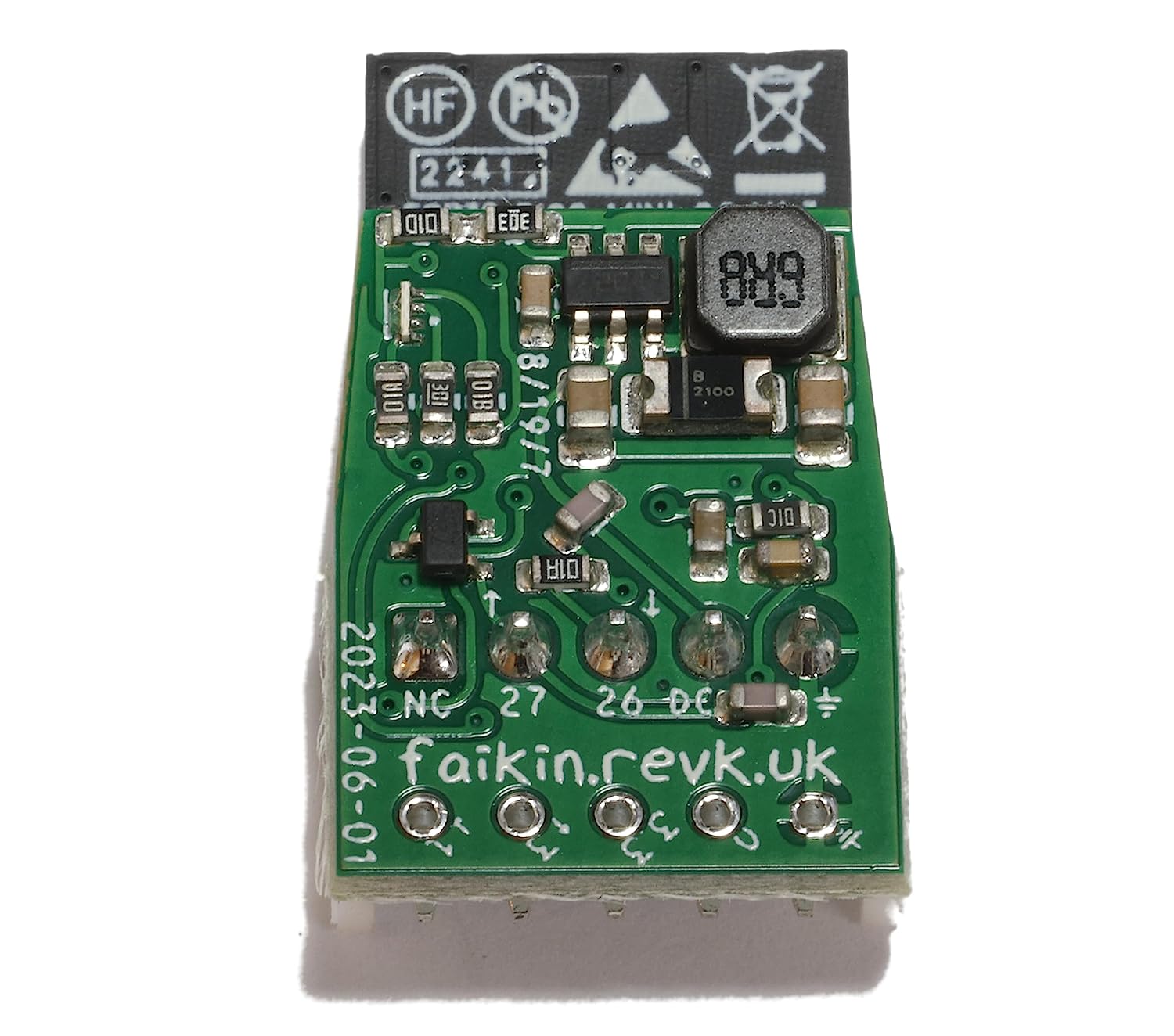
Reading steps is then 4 bytes from 0x1E onwards, low to high bytes for 32 bits.

Resetting the step counter is setting FEATURES_IN(0x47) OR'd 0x04 (self clearing).

2023-07-12

NON-STERLING TRANS FEE

One thing pisses me off is cards charging a Non sterling transfer fee. I'd have expected them to make money on the exchange rate, or be big enough that they can handle currencies without such silly fees to be honest. Even more so when it is someone like American Express, that, well are American, and I am paying something in American dollars. You would think they could handle dollars.

But I have recently discovered something slightly odd.

VISA

Using my VISA debit I was charged...

AMOUNT IN USD 206.87 ON 28 JUN VISA 1.269999 FINAL GBP AMOUNT INCLUDES NON-STERLING TRANS FEE £4.48 = £167.37

But when I was then refunded, it looks like...

AMOUNT IN USD 206.87 ON 30 JUN VISA 1.2669 FINAL GBP AMOUNT INCLUDES NON-STERLING TRANS FEE £4.49 = £158.80

This means I was charged for the refund, and oddly charged at a higher rate (by 1p).

Amex

Using my Amex I was charged... (different day, I have not compared exchange rates)

71.15 UNITED STATES DOLLAR, Non-sterling transaction fee: £1.68, Exchange rate: 1.2687 = £57.76

But when I was then refunded... (next day)

71.15 UNITED STATES DOLLAR = £57.82

Comparison

VISA charge the non sterling fee on charge and refund, but Amex do not. Indeed it seems they effectively refund the non sterling admin fee.

VISAs fee appears to be around 2.7%, Amex fee appears to be around 2.9%, very similar.

Conclusion

It is actually in my companies best interests if I pay for these on my personal Amex and claim on expenses, if there is any chance of a refund (which happens quite a lot if I have arguments with JLCPCB, for example).

2023-07-07

toot

Twice I setup Mastodon.

Once many years ago - I followed the step but step guide and got it working. It worked for quite a while and then broke - out of disk. I gave up.

Then a second time we easier - this time my ops team set me up a VM, and Mastodon had improved a bit, so set up again, following the instructions. Again it worked. It caused problems as it was a "new" instance on an existing domain, and that caused things that had cached stuff to get confused. It got sorted, people had follow requests they had to cancel and try again, that sort of thing.

These days it seems to have a lot more "cleanup" logic, and a lot more obvious on disk usage, but still far from perfect from what I can see.

WTF is it not simple?

My big issue really is that Mastodon should be like apache, or many other quite complex systems, which are basically apt install mastodon. That really is what it should be. Simple as that. The web interface or command line could take you through the initial steps for admin user password and domain name and so on, but that should be it.

There are docker instances. I know nothing about docker, but I am told they sort of just work. Maybe that is the answer?

But why is it not as simple any anything else on linux, really. It seems Ruby is the main problem, as is python it seems. A pain in the arse.

But all is well, so not problem.

Yes, all is well, and even upgrading to next mastodon version as needed was not that hard. Again, following a load of step by step instructions not a simple apt upgrade mastodon or some such. But not rocket science.

But err, then, it broke. Basically the ops team wanted to upgrade Debian to bookworm, which is fair enough, but doing so cleaned out almost all of the stuff Mastodon needs.

Now I am not just upgrading Mastodon, and not installing Mastodon (as I don't want to lose/break what I have), I am sort of trying to make it work from instructions that are one or the other, and constantly hitting stupidities like OpenSSL is not available (how the fuck is that not standard in these tools?!) and not clue how to fix that.

I gave up

I must be getting old, because, yes, I gave up, it is too much of a pain in the arse, and I have better things to do. I tried, honest, but life is too short.

Bring in the experts!

The simple answer is to call in some experts. In this case Mythic Beasts. They actually run the A&A instance because my ops team were smart enough to not go near this with a barge pole.

They are not only running my instance, but in very short order managed to copy all the stuff from the old, and now broken, instance over, and make it continue seamlessly for me, well mostly - some avatar issues they are fixing. But followers, and so on, all working. I have not missed anything and was off for a day at most.

It is not cheap, it is several hundred quid a year. But what do I value my time at?

There is an irony here. I am paying that for my social media. If the likes of Twitter had people paying that for a really good, clean, not sales/advertising/pushy/confrontational/stressy service, they would make a fortune. That is not their business model.

The only mitigation is it may end up being more than just me - some family members, when they finally catch this boat. Of course, subject to whatever stupid rules the Online Safety Bill may create, LOL!

2023-06-29

Pipelining

I am reminded of years gone by when "compiling" would take a long time, even hours in some cases.

This lead to a "pipelined" debugging and development cycle. By the time what you did was compiled you already had fixed a load of bugs and added a load of new features that needed testing. So you had to test things from the compilation as they were when you started. Sometimes you just knew the compilation would create something broken, but some other aspects would be things you need to test, so you let it run anyway to test them. You had to make code that would include things you need to test in the best way possible.

I am sort of doing that with PCBs over the last week or so - getting a new PCB takes slightly over one week from China.

I have been working on a load of small changes to various designs.

  • New 5 pin pad for programming - I made a larger set of holes as the ones on my last batch were annoyingly small and have to be held in place while programming. This is one I finally have back prototypes and my new design is too big and loose, FFS.
  • New New 5 pin pad for programming, staggered more than last time to allow pins and hold them whilst programming - waiting - works perfectly
  • New voltage regulator - waiting - and I really hope it is right as I have several in the pipeline with no fallback - one version works nicely (the cheaper one), the other (tantalum cap) does not work.
  • New USB UART - got a board, discovered I cocked up - but was able to rework some and test the correct design - some boards were able to be used anyway
  • New New USB UART - fixed layout/design issue - waiting - working
  • New RGB LED - waiting, but already spotted that I have cocked up and got G and B swapped, FFS. This means the resistors will be wrong for the colours as well. May be able to rework when this arrives.
  • New New RGB LED - waiting on revised, but still not been able to check if resistors right - waiting - working
  • New panel design - i.e. making part in a 70x70 panel instead of JLC doing it, and if a barcode is clean in silkscreen - waiting - looks nice but JLC being a pain
  • New Tx on Faikin, open drain output - waiting - working
  • New Rx pull to 3V3 on Faikin, detect loopback - waiting

The whole thing is frustrating. I have had to scrap one set of boards sadly because of the CH340X issue. Others I was able to rework, or remove and use a 5 pin programming header instead. One trick is making a new board that you can "fall back" if the new bit does not work.

The RGB LED is a pain - I used one (side mounted) that worked nicely because they did not have the simple one I got from Mouser and used for my hand soldered boards. But JLC places it badly (over 10% of boards needed rework). And I found they had an equivalent simple front facing RGB LED with low enough voltage on the blue for 3.3V working. The issue is the resistors - you can work out values - as I had originally but then find green is way too bright. For my manual working I had changed resistors and so am trying those values to start with. But until I get them, and get the G and B right, I will not be sure I have the right resistors even if I have the right colours. I may have to rework some 0402 resistors to test when they arrive.

On top of it, DHL, who have managed around 2 days from China with no VAT issues, have suddenly made it 3 or 4 days and not doing proper VAT with postponed VAT accounting - that will be a fun argument as I am planning to refuse to pay and insist they re-do as PVA. We will see.

Also JLC being odd on rules, insisting multiple designs on a board even if only in solder resist. Still not resolved. Even if I end up making panels with no extra silkscreen, at least making as panels myself, instead of leaving JLC to do it, lets me make cleaner slots and edges on the designs.

I have to test if the barcode in silkscreen works, and is acceptable (inside a nearly clear, slightly pink, anti static bag) with Amazon - so avoiding having stickers.

So a very frustrating week, and another such week to come.

CH340X DTR/TNOW with ESP8266/ESP32 BOOT and RESET

The CH340X is a small chip that does USB UART, and is part of a family of CH340 chips in various sizes. A UART can need few or many pins, and they do a really small one that is just Rx, Tx and RTS pins, which is the minimum you would want. But they also do a version specially aimed at the needs of small processors like the ESP to handle boot mode.


BOOT and RESET

Both ESP8266 and ESP32 (and many other processors) have a BOOT and RESET input, well, actually GPIO0 and EN.

You need these to program and debug. To program you have to set BOOT MODE, (which is GPIO0 pulled low) and pulse RESET (EN low and then high). For debug, you want no BOOT or RESET, or maybe RESET to restart the processor, but not BOOT mode (GPIO0 staying high).

What is weird is the various ESP based modules out there. I have seen complicated FET based links of RTS and DTR from a UART linked to GPIO0 and EN, and some with R/C combinations linked to RST and GPIO0. I think the logic here is for more traditional use of DTR and RTS, i.e. usually one has RTS active the whole time, so an R/C allows RTS to be activated (low) but EN to pulse low and back high. Similarly linking the use of DTR and RTS to allow a normal UART operation not to be BOOT MODE.

However, the esptool and idf.py as part of the ESP IDF, and even the tasmotizer tool and web page all treat DTR as BOOT MODE and RTS as RESET directly.

You can connect DTR directly to GPIO0 and RTS directly to EN, and it works perfectly!

What is even more weird is the number of modules you see with actual push buttons for BOOT and RESET on the board, which costs money to fit, even though they have a USB UART.

I can only assume some legacy designs and copying reference designs and so on.

All my designs connect DTR to GPIO0 and RST to EN, and work perfectly. Yay.

CH340X DTR

The CH340X has Tx and Rx and also CTS (input) and DTR/TNOW (output).

The TNOW is multi function though, the datasheet says :-

5.3. DTR and multi-mode MCU download

For CH340X, 6# Pin defaults to TNOW, weak pull-up during power-on or reset, output TNOW during normal operation used for half-duplex transceiver switchover. By connecting an external resistor with 6# pin, TNOW can be switch to DTR#, the two options are as follows:

If the 4.7KΩ pull-down resistor is connected to GND with the 6# pin, it will enter the open source DTR enhanced mode, and the 6# pin will automatically switch to the open source driven DTR# pin , which is used to connect the boot mode pin of MCU. The default DTR # is not output and is kept low by the external resistor, but the DTR# pin can be set to output high level or not output by the application program, which is used for multi-mode MCU download with DTR# default low level.

If a 4.7KΩ resistor is connected between the 6# pin and the 5# pin, it will enter the push-pull DTR enhanced mode, and the 6# pin will automatically switch to the push-pull driven DTR# for connecting to

the control pin of the MCU. The application program sets the DTR# pin to output high or low level for multi-mode MCU download with DTR# default high level.

This is excellent, and makes it clear they have considered the use of DTR as a BOOT MODE for processors. I have not tested the DTR to GND via 4k7 - I think they are saying it inverts, i.e. DTR drives high. I may be wrong.

But the second mode, DTR to CTS via 4k7, I have tested. Well, actually I misread / assumed 4k7 to 3.3V, and that does not work, but when 4k7 to CTS it works, and drives the pin as DTR allowing direct connect to GPIO0 yay

Why a 4k7?

But I am puzzled. I understand the 4k7 to GND, as it pulls down, and allows active drive high as needed. But why 4k7 to CTS.

CTS is an input, so the only use of the link is to allow the CH340 to confirm the connection from DTR/TNOW (output) to CTS (input). Indeed, it pulses that output low a few milliseconds after startup, presumably to test it is connected to CTS.

The thing that puzzles me is why the 4k7. With CTS as an input it is quite safe and valid to connect DTR directly to CTS, output to input. And, as you would expect, doing that causes the CH340X to switch in to DTR output mode.

I suppose one could argue that you may want to make use of CTS as well, and the 4k7 allows that even if DTR is outputting something different. Except that does not work. If you are using CTS, that means you have an active signal feeding CTS from somewhere. If that is the case, the test of DTR to CTS does not work (I tried it!) as CTS will not see the signal from DTR/TNOW via the 4k7. So the 4k7 does not allow that. Indeed, the only use may be if you have something driving CTS which does not drive it at power up - that would be a rather special arrangement and somewhat unlikely. That said, I suppose if CTS was a general purpose GPIO from a CPU which starts as floating/input, it could make sense and allow CTS to be signalled from the CPU.

So I'd expect the data sheet to say just link DTR to CTS and not use CTS, or use 4k7 if CTS is floating at power up and needs to be used.

Anyway I have done that (just linked DTR to CTS), and it works nicely.

USB-A tracks to CH340X

There is a snag though - using DTR to drive GPIO0 works, but on my Shelly board it is drive GPIO0 that is connected internally in the board, with some pull something, and an LED, and so on. So the CH340 might "see" the pull down on it when it starts perhaps. So I have to drive through a buffer in that case. Thankfully that is basically the only case, as normally it just goes directly to GPIO0 on the connected ESP module.

2023-06-28

JLCPCB and fun rules

I am using JLCPCB for my small boards. There are other places, but they seem reasonably sensibly priced, have a good automated ordering process, and are quite quick.

However, I have been trying to do something clever, and that is always a bad idea.

If I have a small circuit board, and want assembly, they will make it in to a small panel, e.g. 70x70m, with "rails" top and bottom, and V-cuts. This means when you get it, it snaps out of the 70x70mm PCB. The rails have some holes and fiducials.

As it happens, I am shipping (to Amazon) as a 70x70mm panel. This is partly because it fits better in a small anti-static bag, and partly to make clear it is sold as a component, an assembled PCB, and not a final product with UKCA/CE, etc. As it happens the main module is CE marked, with a RF can, and the only extra bits are normally just a small voltage regulator, so getting UKCA/CE marked should not be too hard one day, but for now, these are hobbyist projects.

Anyway, the 70x70mm panel has loads of wasted space. JLC add an order number (unless you pay them extra not to), but other than that, just unused blank PCB, a few holes, and fiducials.

So I decided to try and make use of it - make the 70x70mm panel myself. They allow this and have instructions for where to put fiducials. They also seem to want some holes and instructions seem to be lacking for those, but I copied what they did. However, this created a few challenges :-)

V-Cuts

The first problem is the V-cuts are cuts in to the board at the last stage, and always go right across the board (they explain this), but can go any direction (well, at least up/down or left/right). These allow the small PCBs to be snapped out. Some extra milling around bits of the PCB that are not simple straight edges allows other shapes, so works well.

For example, this is what they did when ordered simply as a tiny PCB. Four V-cuts to snap out.

KiCad

Firstly, how to tell KiCad. I cannot simply put these on the Edge.Cuts later as it would break the board outline - KiCad would fail DRC and not show the board on the 3D view and so on. So simple answer is a separate layer, easy enough.

But then KiCad does not know, for example, that tracks and copper fill should not get too close to these V Cuts. It knows for edge cuts, and so one can have milled slots for non rectangular edges, but the V cuts are not seen.

My solution was to make a footprint that is a 70mm V-cut.

  • 70mm line on User.1 layer as the actual V-Cut
  • Line on User.Comments and Fab layers to more visible
  • A courtyard for 1mm above the V cut on one side
  • An exclude for 0.2mm either side, front and back

The exclude keeps tracks and pads and so on away, just like Edge.Cuts.

The courtyard works on the basis that you have to bend the PCB to snap it, and that could be up or down. I have parts that hang over the edge (the antenna of the ESP32 module, etc), but by adding a courtyard one side I ensure I cannot accidentally have things hanging over the edge both sides. I have to flip the V-cut footprint to fit, but it allows a sane DRC.

Telling JLCPCB

This took a few attempts to get right.

For a start, I updated the JLC-Plugin to export an extra file for V.Cuts - I just added to the config file, and it exported. The problem though is that, even as a file called V_Cuts, it shows as a User.1 layer when viewed, and apparently this would mean adding a note to the order so they don't miss it. I don't trust myself to add a note.

However, after a few emails back and forth, I found that what they really wanted was V Cuts simply included in the Edge.Cuts file. It breaks some of the preview stuff as not a joined up border, but it is understood by their people it seems, and won't be missed.

I have done a MR on the plugin to include the User.1 in the Edge.Cuts file as part of the export, so I don't have to think about it.

Extra artwork on the panel

Adding extra artwork to the panel was pretty simple - just more silk screen. What took slightly more work is I wanted a barcode, and so made a tool to create a KiCad barcode module.

Then I ordered.

They I got a "we want $50 more" response. They said it was 3 designs. Actually, by their rules it was 5.

FFS

So, the rule is, if you have parts that detach, and they have any traces or silkscreen, they are treated as additional "designs" on the same order, and there is a surcharge for each extra design. So even a "design" that is just text on silk screen has a surcharge.

Simpler

A simple step was only silk screen on one of the unused parts, that made it 2 designs. So progress.

The problem is that the surcharge, whilst only $2 on the PCB manufacturer, they also surcharge the assembly, by around $30. Now I have queried as, even if there are 2 designs, I only want one assembled - the one with components on it.

It may be possible to order PCB as 2 designs and then order assembly as 1, but I cannot see any way to actually do that, sadly.

Solder resist

Another trick may be to avoid the multiple designs by following the rules. The rules cover tracks and silkscreen. Well, it seems we can do solder resist. Using this on an FR4 board with black solder resist may well have enough contrast. Even more so if copper fill and ENIG finish.

It needs more testing to see what resolution and contrast is achievable.

The latest attempt...

This is 2 designs because of the silk screen. But testing they agree with that by having the solder resist at the top as well.

Update: They magically decided this was 5 designs so I have challenged as "solder mask/resist" is not something they list as creating extra designs. We'll see...

Update: They seem to be doubling down on the "5 designs" still. I asked if the rules have changed?


Update: They are sticking to their rules, but making up bullshit for them, saying that they have to "load two programmes" if it is two designs. This is clearly bullshit, but I have challenged on basis that they do put their order number on silkscreen on one of the snap of panels, so extra silkscreen on that panel will be no more work, will it, as they are "loading two programmes" already, for their order number. We'll see.

2023-06-16

To USB or not to USB, that is the question!

I have done quite a lot of small boards now, as I have blogged at various points.

It has helped me build up my skills in circuit and PCB design, and over time I have moved to different approaches for things as I have learned. Some things driven by practical usage, some by cost, some by simplicity.

At present I am working on ESP32 based boards, and I may yet move on to ESP32-S2 or ESP32-S3, at least one of which does some direct USB, but for now, for ESP32, I need serial connection for programming and debug. The ESP32 are especially appealing in the form of the ESP32-PICO-MINI-02 module which has extra flash and RAM which is invaluable.

I have "standardised" on a USB-C connector for my boards, where needed, for simple power. That is most boards, e.g. this LED strip controller.

It uses USB-C for the 5V supply for the LED strip, and via 3.3V regulator for the ESP32.

In many designs, I have included an FT231XQ USB UART in the design, allowing not just power, but programming and debug via the USB-C connector. This works really well. It makes it very simple to develop on. I have even learned my lesson with diodes on boards which can also have 12V DC, and USB connecting both at the same time :-)

But the FT231XQ is not a cheap part, and not a readily available part (a lot of parts are now available after COVID, but some still in very short supply). So I have been making even these boards have an alternative for when the FT231XQ cannot be fitted.

Indeed, I have actually started making boards which have no FT231XQ at all, even if they have a USB-C socket for power (like the one shown above).

This means I need some sort of header. One of the reasons I went with the UART in the first place is any sort of sensible header connector would take as much board space as the UART chip, and add cost or time, especially if a through hole connector.

But, the way Shelly do it has come to the rescue. They use a small 1/10" 5 pin header (and a 1/20th" 7 pin header) - a socket on the board, and I made this to work with them. These are useful if you are wanting to reprogram Shelly with say tasmota, or for any projects with similar devices. See Amazon.

It has header pins for the 5 and 7 way connectors. The shelly has a proper socket for these.

However, I can simply make the board have holes, instead of a proper "header", like the 5 holes on this boards.

I can simply push the pins in the holes, and hold them whilst programming. Indeed, if I can get the holes just right they will fit firmly enough not to need holding and so can be used for debug as well. It is cheap - holes don't really cost anything. It does not take a lot of space, especially as it can (like that example) be under another connector even.

I am working on slight variations of the holes, to try and make a firm fit to the square pins. The latest is slotted holes. In practice this means each set of boards I get has a slight improvement and I try it. The above design had holes slightly too small - some boards needed to be "held" whilst programming (which is not really a problem, but adds some time). This is my latest design for them.

So it is a question of whether I bother with a UART on future boards. Using USB-C for power is a good idea for a lot of boards - the "Faikin" being one of the few cases where that is not sensible as it fits and existing connector with power. If I move to ESP32-S3 for example, I'll see if that can do USB sensibly directly, but I want a module like the ESP32-PICO-MINI-02 really - not sure if there is one yet.

Oh, and as you may notice, I have adopted a policy of GPIO numbers on silkscreen - it really is damn useful when you have so many generations of so many PCBs lying around. I don't do a lot of silk screen - i.e. no R1, R2, etc, but I have to do some to stop JLCPCB asking questions about pin 1. But GPIOs is invaluable. And now KiCad allows proper fonts it is slightly more fun (the above has "faikin.revk.uk" in xkcd script, err, because I can).

Update: As suggested (and as per above image) I have now gone for staggered pins, to see how that goes.

Update: The silk screen does not work that small, so going for something simpler...

Update: I am also, as someone suggested, trying a CH340X which is physically a similar size for the FT231XQ but a lot cheaper and simper to wire up.

Superimposed CH340X (green) on FT231XQ

Design for USB-A ESP32-PICO-MINI-02 with RGB LED and CH340X

Update: Fuck sake, read the data sheet. 4k7 from CTR to DTR/TNOW is needed, not 4k7 from 3V3 to DTR/TNOW. Sadly meant some boards could not even be reworked. But was able to test this for future boards.

QR abuse...

I'm known for QR code stuff, and my library, but I have done some abuse of them for fun - I did round pixels  rather than rectangular, f...