I am reminded of years gone by when "compiling" would take a long time, even hours in some cases.

This lead to a "pipelined" debugging and development cycle. By the time what you did was compiled you already had fixed a load of bugs and added a load of new features that needed testing. So you had to test things from the compilation as they were when you started. Sometimes you just knew the compilation would create something broken, but some other aspects would be things you need to test, so you let it run anyway to test them. You had to make code that would include things you need to test in the best way possible.
I am sort of doing that with PCBs over the last week or so - getting a new PCB takes slightly over one week from China.
I have been working on a load of small changes to various designs.
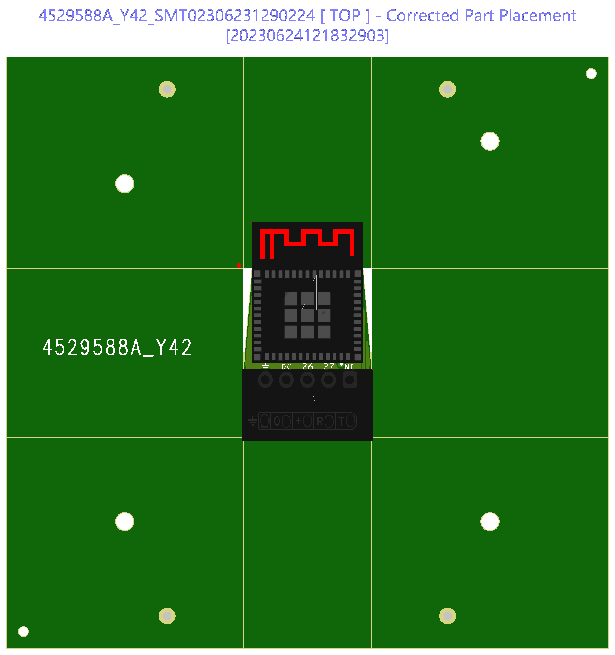
- New 5 pin pad for programming - I made a larger set of holes as the ones on my last batch were annoyingly small and have to be held in place while programming. This is one I finally have back prototypes and my new design is too big and loose, FFS.
- New New 5 pin pad for programming, staggered more than last time to allow pins and hold them whilst programming -
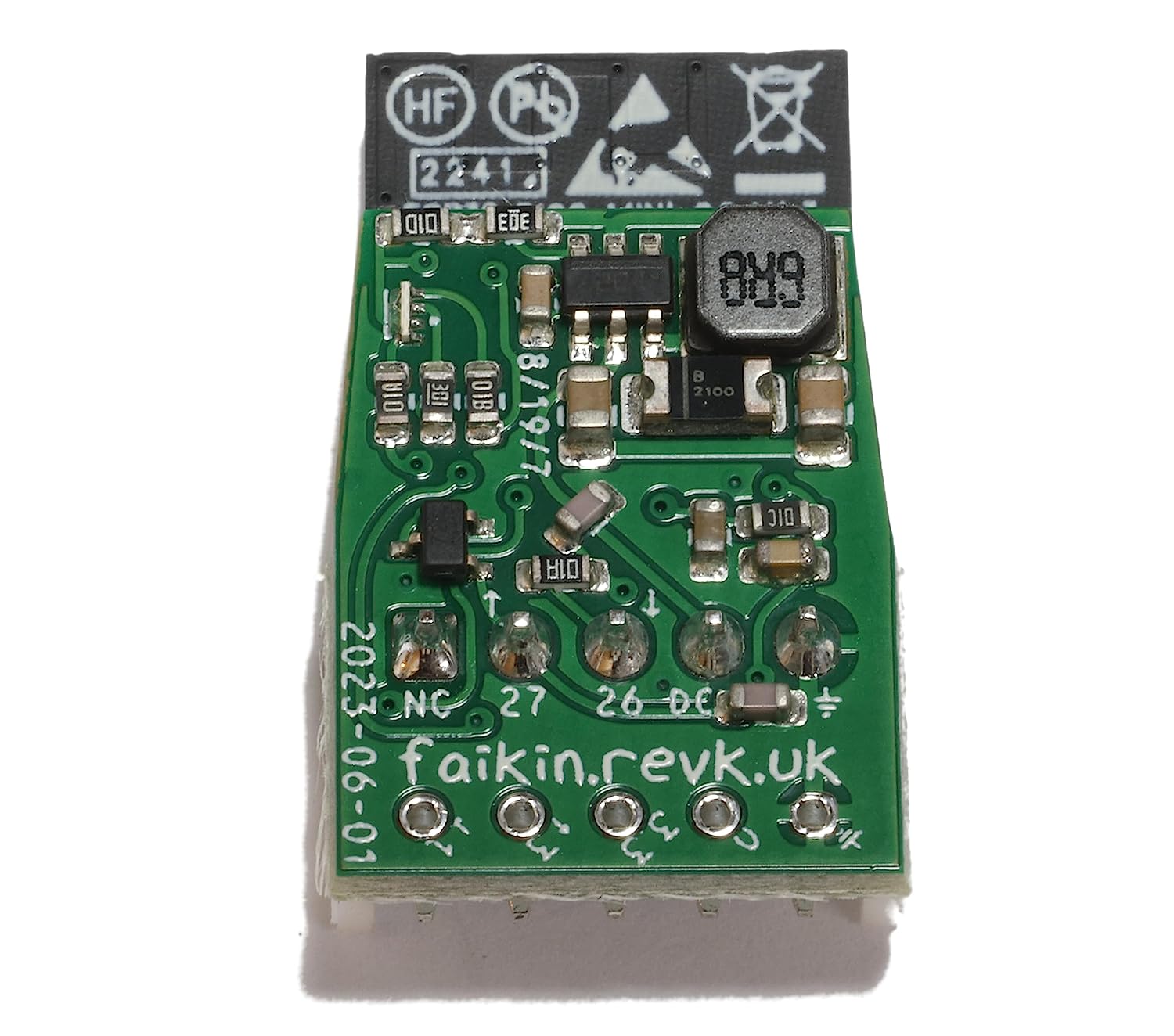
waiting- works perfectly - New voltage regulator -
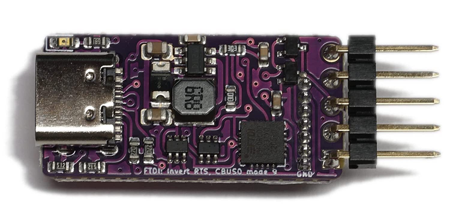
waiting- and I really hope it is right as I have several in the pipeline with no fallback - one version works nicely (the cheaper one), the other (tantalum cap) does not work. - New USB UART - got a board, discovered I cocked up - but was able to rework some and test the correct design - some boards were able to be used anyway
- New New USB UART - fixed layout/design issue -
waiting- working - New RGB LED - waiting, but already spotted that I have cocked up and got G and B swapped, FFS. This means the resistors will be wrong for the colours as well. May be able to rework when this arrives.
- New New RGB LED - waiting on revised, but still not been able to check if resistors right -
waiting- working - New panel design - i.e. making part in a 70x70 panel instead of JLC doing it, and if a barcode is clean in silkscreen -
waiting- looks nice but JLC being a pain - New Tx on Faikin, open drain output -
waiting- working - New Rx pull to 3V3 on Faikin, detect loopback - waiting
The whole thing is frustrating. I have had to scrap one set of boards sadly because of the CH340X issue. Others I was able to rework, or remove and use a 5 pin programming header instead. One trick is making a new board that you can "fall back" if the new bit does not work.
The RGB LED is a pain - I used one (side mounted) that worked nicely because they did not have the simple one I got from Mouser and used for my hand soldered boards. But JLC places it badly (over 10% of boards needed rework). And I found they had an equivalent simple front facing RGB LED with low enough voltage on the blue for 3.3V working. The issue is the resistors - you can work out values - as I had originally but then find green is way too bright. For my manual working I had changed resistors and so am trying those values to start with. But until I get them, and get the G and B right, I will not be sure I have the right resistors even if I have the right colours. I may have to rework some 0402 resistors to test when they arrive.
On top of it, DHL, who have managed around 2 days from China with no VAT issues, have suddenly made it 3 or 4 days and not doing proper VAT with postponed VAT accounting - that will be a fun argument as I am planning to refuse to pay and insist they re-do as PVA. We will see.
Also JLC being odd on rules, insisting multiple designs on a board even if only in solder resist. Still not resolved. Even if I end up making panels with no extra silkscreen, at least making as panels myself, instead of leaving JLC to do it, lets me make cleaner slots and edges on the designs.
I have to test if the barcode in silkscreen works, and is acceptable (inside a nearly clear, slightly pink, anti static bag) with Amazon - so avoiding having stickers.
So a very frustrating week, and another such week to come.